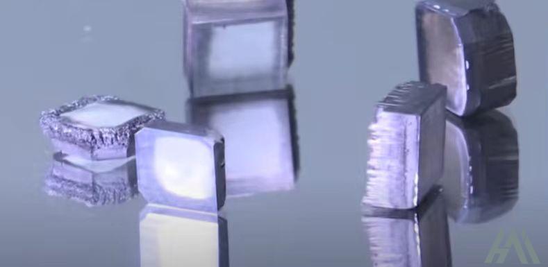
At present, synthetic single crystal diamonds methods can be divided into two categories: high temperature high pressure method (HTHP), chemical vapor deposition method (CVD). The single particle size obtained by HTHP method is relatively small, and the single crystal synthesized by HTHP method may contain impurities such as catalysts, and can not be doped effectively. Chemical vapor deposition (CVD) is a common preparation method of thin film materials, which uses the vapor precursor to deposit the required thin film materials on a specific substrate under specific conditions. In the preparation of single crystal diamond materials, usually used as methane and hydrogen as precursors, under high temperature (about 1000℃), atmospheric pressure (1 atmospheric pressure) or low pressure conditions, with single crystal diamond substrate as the substrate, in the way of gas phase epitaxial growth of single crystal diamond, the single crystal diamond substrate used can be natural diamond, HPHT diamond or CVD diamond.
According to scientists at the Key Laboratory of Marine New Materials and Application Technology of the Chinese Academy of Sciences, the process of cultivating diamond is like growing food, "First of all, there must be a seed chip, but also need to use methane gas, methane under the action of energy, formed a carbon plasma, the plasma is like dust, slowly deposited in the air to the diamond seed chip," Little by little."
Advantages of CVD diamond in semiconductor field The appearance and composition of CVD diamond are almost the same as natural diamond, and the physical and chemical characteristics are not much different, and no difference can be seen between the two under the naked eye. However, the reason why CVD diamond is valued, the most important reason is "pure", it is more clean than natural diamond, almost no impurities. The extremely high purity makes CVD diamonds more likely to be used than natural diamonds - for example, thanks to their excellent electrical properties, diamond materials are now leading the way in the semiconductor field. Diamond and c-BN (6.4eV), Ga2O3 (4.8eV), AIN (4.eV) and other materials with bandgap width of about 5eV, both belong to the current hot ultra-wide bandgap semiconductor materials. Among them, the band gap of diamond is 5.47eV, which is the widest material in the current simple semiconductor materials, and its electrical properties are extremely excellent:
Excellent electrical properties ① Extremely high breakdown electric field: up to 109Vem-1, which is 17 times that of gallium baside material, 2 times that of gallium nitride material, and 2.5 times that of silicon carbide material. 2 saturated carrier speed: in terms of saturated carrier speed, diamond is 2.7 times that of silicon and gallium arsenide, and the carrier speed is larger than the peak value of gallium foundation, that is, it can also maintain its high rate when the field strength increases. ③ Carrier mobility: diamond electron mobility and hole mobility are better than other semiconductor materials, electron mobility at room temperature is 4500cm2/V·S, silicon is only 1500cm2/V·S, gallium arsenide is 8500cm²/ v-s, gallium nitride is less than 1000cm2/V·S; The hole mobility of diamond is 3800cm2/V·S, while silicon is only 600cm2/VS, gallium arsenide is 400cm2/V·S, and gallium nitride is <50cm2/V·S. Therefore, diamond can make high-frequency electronic devices. 4 Low dielectric constant: the dielectric constant of diamond is 5.7, about half of gallium arsenide and less than half of InP, that is, at a given frequency, diamond semiconductors have superior capacitive loads, which provides great convenience for the design of millimeter wave devices. Comparison of basic properties of four semiconductor materials In the semiconductor field, the potential of the most mainstream silicon materials has basically been tapped to the extreme, and better materials are needed to make connections. With all these advantages, CVD diamond really has the opportunity to become the next generation of semiconductor material, can make electronic products run faster, but also more heat resistant, less prone to damage. Scientists believe that future quantum computers may rely on chips made of diamond to greatly improve the thermal conductivity of the computer, so that the computer can maintain smooth operation at close to absolute zero. CVD diamond development goals However, no matter what industry, it is not easy to replace the original production mode and use new raw materials, and it takes time to develop. Diamond to be used in the semiconductor industry, the premise is to produce a larger size of the single crystal material, so by improving the preparation process to produce a larger size of CVD diamond is the main development goal of the industry. With the advancement of manufacturing technology and the reduction of costs, synthetic diamond is expected to lead to a new generation of semiconductor technology revolution.